- 您现在的位置:买卖IC网 > Sheet目录2007 > LV5609LP-TE-L-E (ON Semiconductor)IC CLOCK DRIVER VERT VCT24
32207 MS PC 20060719-S00002 No.A0692-1/8
http://onsemi.com
Semiconductor Components Industries, LLC, 2013
August, 2013
LV5609LP
Overview
The LV5609LP is vertical clock driver for CCD.
Functions
Ternary output ×2ch
Binary output ×2ch
SHT output ×1ch
Output ON resistance : 30Ω typ
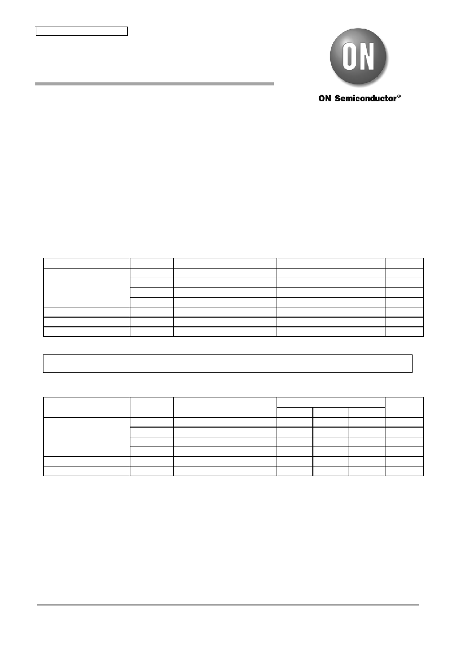
Specifications
Absolute Maximum Ratings at Ta = 25
°C, VSS = VM = 0V
Parameter
Symbol
Conditions
Ratings
Unit
VDD max
6V
VH max
20
V
VL max
-10
V
Maximum supply voltage
VH-VL max
24
V
Allowable power dissipation
Pd max
with specified substrate *
0.8
W
Operating temperature
Topr
-20 to +80
°C
Storage temperature
Tstg
-40 to +125
°C
* : Specified substrate : 40
×50×0.8mm3, glass epoxy four-layer (2S2P) board
Allowable Operating Ratings at Ta = 25
°C, VSS = VM = 0V
Ratings
Parameter
Symbol
Conditions
min
typ
max
Unit
VDD
2.0
3.3
5.5
V
VH
15
17
V
VL
-8.5
-7.5
-4
V
Supply voltage
VH-VL
23.5
V
CMOS input High voltage
VINH
0.8VDD
VDD
V
CMOS input Low voltage
VINL
-0.1
0.4
V
Bi-CMOS LSI
Vertical Clock Driver for CCD
Ordering number : ENA0692
Stresses exceeding Maximum Ratings may damage the device. Maximum Ratings are stress ratings only. Functional operation above the Recommended Operating
Conditions is not implied. Extended exposure to stresses above the Recommended Operating Conditions may affect device reliability.
发布紧急采购,3分钟左右您将得到回复。
相关PDF资料
M-986-2A1PL
IC TRANSCEIVER MF 2CHAN 44-PLCC
MAX038CWP+
IC GEN WAVEFORM HI-FREQ 20-SOIC
MAX1002CAX+T
IC ADC 6BIT 60MSPS DUAL 36-SSOP
MAX1003CAX
IC ADC DUAL 6-BIT 90MSPS 36-SSOP
MAX1011CEG+
IC ADC 6BIT 90MSPS 24-QSOP
MAX105ECS+T
IC ADC 6BIT 800MSPS DL 80TQFP
MAX1063AEEG+
IC ADC 10BIT 250KSPS 24-QSOP
MAX107ECS+
IC ADC 6BIT 400MSPS DL 80-TQFP
相关代理商/技术参数
LV5609V
制造商:SANYO 制造商全称:Sanyo Semicon Device 功能描述:Bi-CMOS LSI For CCD Vertical Clock Driver
LV5609V-HAS-TLM-E
功能描述:时钟驱动器及分配 RoHS:否 制造商:Micrel 乘法/除法因子:1:4 输出类型:Differential 最大输出频率:4.2 GHz 电源电压-最大: 电源电压-最小:5 V 最大工作温度:+ 85 C 封装 / 箱体:SOIC-8 封装:Reel
LV5609V-MPB-E
功能描述:时钟驱动器及分配 RoHS:否 制造商:Micrel 乘法/除法因子:1:4 输出类型:Differential 最大输出频率:4.2 GHz 电源电压-最大: 电源电压-最小:5 V 最大工作温度:+ 85 C 封装 / 箱体:SOIC-8 封装:Reel
LV5609V-TLM-E
功能描述:时钟驱动器及分配 RoHS:否 制造商:Micrel 乘法/除法因子:1:4 输出类型:Differential 最大输出频率:4.2 GHz 电源电压-最大: 电源电压-最小:5 V 最大工作温度:+ 85 C 封装 / 箱体:SOIC-8 封装:Reel
LV-560M2W---2025S
制造商:Surge Components Inc 功能描述:CAP ALUM 56UF 450V ?20% 2000LHRS 20 X 25 - Bulk
LV560MCRO
制造商:未知厂家 制造商全称:未知厂家 功能描述:Analog IC
LV560PLID
制造商:未知厂家 制造商全称:未知厂家 功能描述:Analog IC
LV-561M2G---3545S
制造商:Surge Components Inc 功能描述:CAP ALUM 560UF 400V ?20% 2000LHRS 35 X 45 - Bulk